找回密碼
 新用戶註冊
搜索
熱搜: hifi av 音樂
查看: 12001|回復: 19

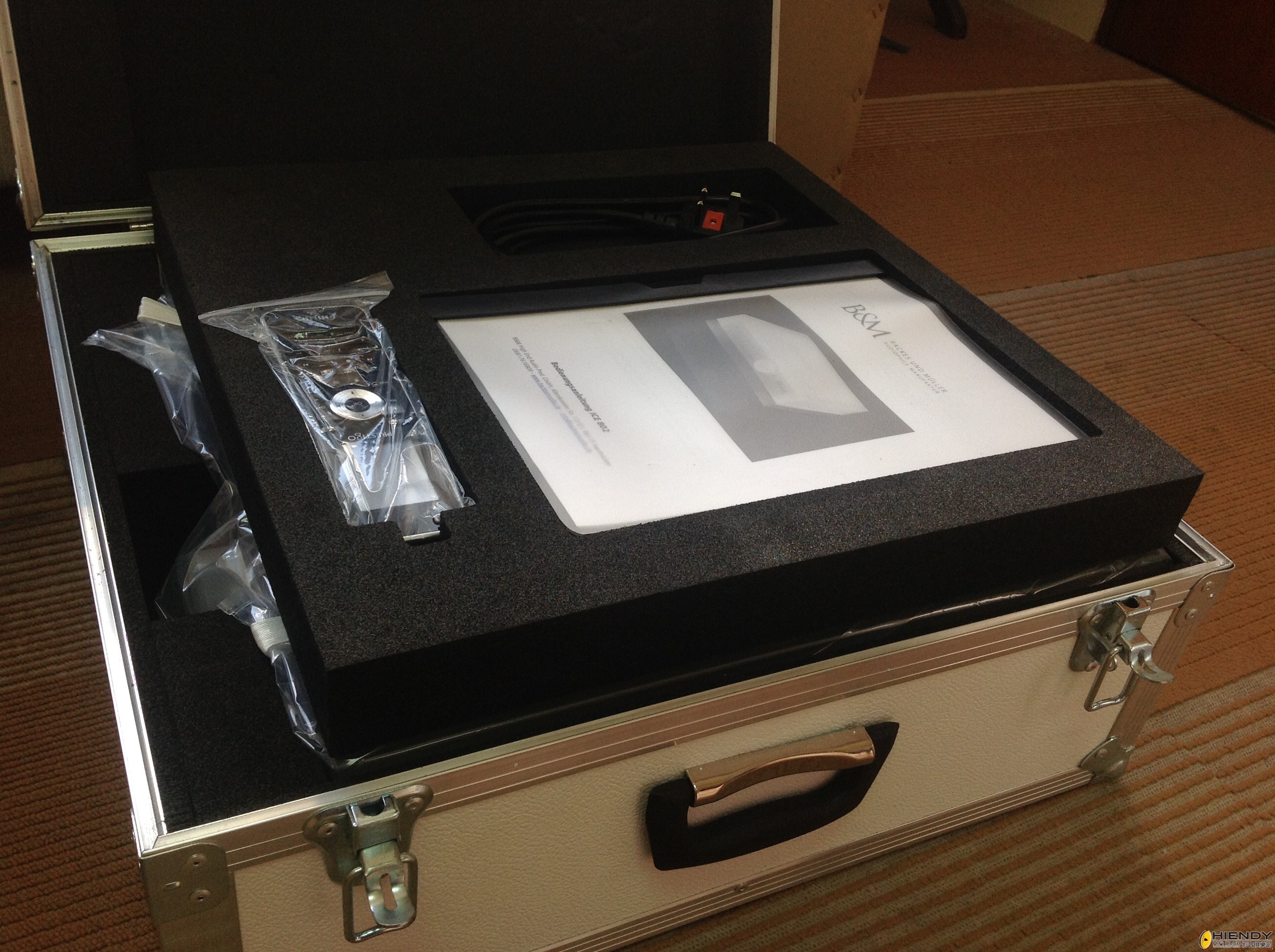
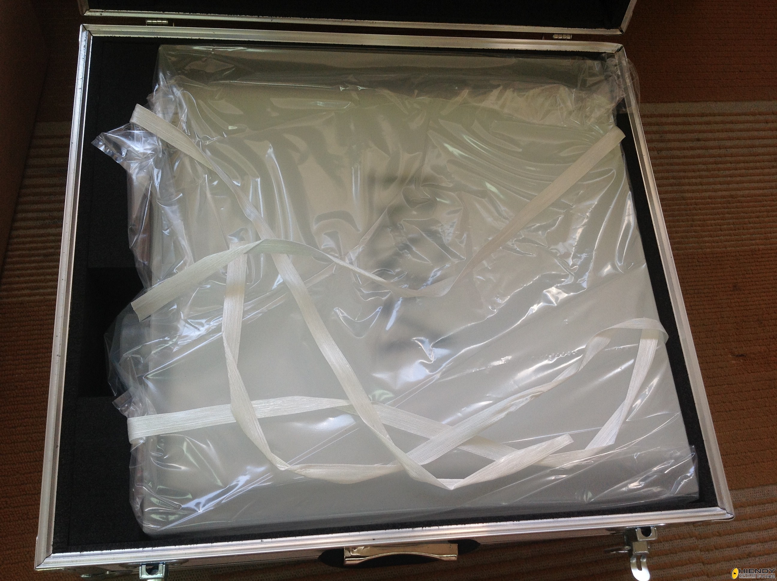
[CAS] Backes & Muller ICE 802 開箱

[複製鏈接]
發表於 2014-1-15 15:19:24 | 顯示全部樓層 |閱讀模式
本帖最後由 hkborn 於 2014-1-15 15:21 編輯

Image - 2014年1月15日 14.50.12.jpg
Image - 2014年1月15日 14.50.53.jpg
Image - 2014年1月15日 14.51.37.jpg
Image - 2014年1月15日 14.54.46.jpg
Image - 2014年1月15日 14.55.29.jpg
Image - 2014年1月15日 14.57.01.jpg
Image - 2014年1月15日 14.57.16.jpg
Quote from Linn Forum:
http://forums.linn.co.uk/bb/showthread.php?tid=24975
BM Line series and BM ICE media device
Howdy,

is there anyone familar with the Backes and Müller Line series and their BM ICE media device?

It appears Backes and Müller have been using a similar concept for several years now that Linn are introducing with the Exact system.

I also heard of a number of Klimax owners (350 plus DS) who switched to BM line plus BM ICE.

Considering both combinations I'f be very much interested in first-hand experiences.

Thanks.

評分

2

查看全部評分

 樓主| 發表於 2014-1-15 15:44:19 | 顯示全部樓層
本帖最後由 hkborn 於 2014-1-15 15:47 編輯

上網才看到Linn Forum說有Klimax 350用家轉用B&M Line+ICE; Klimax 350 定價在50000鎊,與之相若的B&M應是BM35,也是KSDigital的Line Master 。
看來有源音箱已經開始為傳統發燒友接受。
回復

使用道具 舉報

 樓主| 發表於 2014-1-15 15:53:07 | 顯示全部樓層
回復

使用道具 舉報

發表於 2014-1-15 16:04:26 | 顯示全部樓層
hkborn 發表於 2014-1-15 15:44
上網才看到Linn Forum說有Klimax 350用家轉用B&M Line+ICE; Klimax 350 定價在50000鎊,與之相若的B&M應 ...

好靚仔但  定價在50000鎊..大拿拿....HK$50萬
回復

使用道具 舉報

 樓主| 發表於 2014-1-15 16:07:19 | 顯示全部樓層
馬丁 發表於 2014-1-15 16:04
好靚仔但  定價在50000鎊..大拿拿....HK$50萬

唔系,呢部定價在十萬左右
回復

使用道具 舉報

發表於 2014-1-15 16:15:49 | 顯示全部樓層
hkborn 發表於 2014-1-15 16:07
唔系,呢部定價在十萬左右

E加D機靓仔D.靓聲D的都開10個.
回復

使用道具 舉報

 樓主| 發表於 2014-1-15 16:21:18 | 顯示全部樓層
回復

使用道具 舉報

發表於 2014-1-15 16:23:29 | 顯示全部樓層
B&M冇認識, 不過睇包裝十皮唔算貴


.....雖然我都買唔起
回復

使用道具 舉報

 樓主| 發表於 2014-1-15 19:48:05 | 顯示全部樓層
貴與不貴見仁見智。
按功能說,它是高階前級和解碼,模擬可接入rca及xlr;數碼則有光纖,RCA,xlr接口。
除專業產品外,家用音響只有入門產品有如此多功能,但質素有限。

回復

使用道具 舉報

發表於 2014-1-15 22:19:51 | 顯示全部樓層
本帖最後由 JSL 於 2014-1-15 22:22 編輯

Judging from the open-case picture of ICE502, this is a surprisingly "clean" machine? Can you please share more information about the difference between ICE502 and ICE802? Thanks


Setting aside the debate of design complexity, I have to admit that casing and styling of this machine is very impressive


ICE502.jpg

評分

1

查看全部評分

回復

使用道具 舉報

發表於 2014-1-15 22:57:42 | 顯示全部樓層
包裝相當吸引,希望將成本放在音質設計上,不竟器材還是音質先決。
121032g5wye5lpleweweb3.gif
Emoji_140535.png
Emoji_140545.png
Emoji_140558.png
回復

使用道具 舉報

 樓主| 發表於 2014-1-15 23:49:52 | 顯示全部樓層
main difference between 502 and 802 in that
1) the latter has a tube stage

The  ICE 802 that sets it apart from the usual variants.
A conventional tube circuit has principle related technical disadvantages. Depending on the gain or power, the operating points vary during operation and can hardly be kept stable.
The analog tube output of the ICE 802 is equipped with selected ECC82 tubes.
ß = 1
The tube does not increase at the ICE 802, because the volume control happens on the upstream transistor stage.
The gain of the tube is always 1
The signal noise could be reduced this circuit technique on since then not known values.
The life of the tube is increased by an electronic soft start of the heating voltage.
2) it has direct volume control on B&M high end models, benefit being
"Volume control in perfection:
For large models BM Line 25, Line 35 BM, BM Line 50, Line 100 BM the volume control is done by changing the gain of all individual drivers in the speaker.

This means the voltage present at the digital input data stream will not be reduced in its word width. It passes through the entire digital signal processing, without changing the bit pattern, and thus the music content.

The volume control is analog, directly to the amplifiers. The magnitude of the gain determines the volume at which the music is played.
UNIQUE
This type of volume control is unique. Only Backes & Müller speakers are due to their complex, sophisticated structure through the so-called VCA."

回復

使用道具 舉報

 樓主| 發表於 2014-1-15 23:58:48 | 顯示全部樓層
smalltiger 發表於 2014-1-15 22:57
包裝相當吸引,希望將成本放在音質設計上,不竟器材還是音質先決。  ...

traditionally, B&M is focused on active speakers for audiophile market, KS Digital being the studio arm.
this media server is designed for line series active speakers to make them a complete set of sound playback system.
price range of line series speakers spreads from $300,000 to over a million, so $100,000 isn't that expensive.
回復

使用道具 舉報

 樓主| 發表於 2014-1-17 01:56:00 | 顯示全部樓層
今天接駁好ice 802,  主要是將不同播放器連接到ice, 然後再直出Line Master 有源音箱。系統主體是ice 及一對有源音箱,幾乎所有音源都可輸入,看電視,聽黑膠,用電腦看片,看u-tube, 聽數碼收音。。。
ICE(2).jpg
回復

使用道具 舉報

 樓主| 發表於 2014-1-17 12:32:00 | 顯示全部樓層

Understanding Temperature Drift in a Precision Digital-to-Analog Converter (DAC)
By:          David Fry, Strategic Applications Engineering Manager
May 10, 2012

Abstract: This application note analyzes the external influences that introduce error to a precision digital-to-analog converter (DAC). Focus will be on temperature drift. This error is recognized as part of a DAC's error budget. The article discusses the error factors introduced by both the data converter and the voltage reference. After understanding the sources of error, it then provides the calculations required to specify the data converter and that will compensate for the error and meet a system's target specifications.

This application note focuses on Maxim's 3-terminal voltage references and precision DACs. Voltage references and DACs have many specifications, but only those relevant to the error budget will be discussed.

Overview
An ideal digital-to-analog converter (DAC) produces an analog output voltage or current that is perfectly linear and independent of many external influences such as temperature. That said, DACs are, of course, subject to errors caused by many external factors, notably temperature. As temperature varies, the DAC can drift. This is of particular importance when a precision DAC is used to set a precise bias value. Any error can be calibrated out at room temperature. However, variations with temperature are far more difficult to compensate for. The errors that drift most with temperature are dominated by offset error and gain error.
This application note describes how DAC offset and gain errors are specified with temperature. It shows how a designer can anticipate the errors in the design process. Once understood, this knowledge can be used to ensure that a system meets its required specification over temperature.
Offset and Gain Errors
As stated above, DAC performance is affected by many sources of error including offset error and gain error. These factors are specified in the "Static Accuracy" section of a DAC's data sheet. An example is shown in Figure 1 for the MAX5134 16-bit, quad DAC.
Figure 1. MAX5134 offset and gain errors.
Note 4: Gain and offset tested within 100mV of GND and AVDD.
Figure 1. The MAX5134 offset and gain errors.
What do these specifications really mean for DAC performance?
Offset error defines how well the actual transfer function of a DAC matches the ideal at a single point. For a unipolar output, this is at code zero. This error is often called zero-code error. For a bipolar output, this is at the point where the DAC output should pass through zero.
Gain error is a measure of the slope of the transfer function. In the example device, the slope can be between 99.5% and 100.5% of ideal.
Ideal offset and gain errors are shown in Figure 2. Note that offset and gain errors can be both positive and negative.
Figure 2. Offset and gain errors.
Offset and gain errors are not generally measured directly. If a unipolar device exhibits a negative offset error, then measuring at code zero will give an erroneous result. The explanation for this is actually straightforward. Theoretically, with a negative offset error the output should be negative at code zero. A unipolar DAC cannot do that, since it generally only has a positive supply. Thus, two points are measured and the offset and gain errors are calculated. One point is close to code zero while the other is close to, or possibly at, maximum code. The MAX5134, for example, is tested within 100mV of ground and AVDD; the analog supply voltage as described in Note 4 of Figure 1.
Now consider the influence of temperature. Both offset and gain errors drift with temperature. This is of particular importance where a DAC is used to set precise bias values. Fixed-offset and gain error can be calibrated out using various techniques. (See application note 4494, "Methods for Calibrating Gain Error in Data-Converter Systems," for some ideas on this.) However, calibrating out temperature drift is far more complex since temperature must first be measured and a variable compensation applied dependant on temperature.
Example Calculations and Typical Results
Using the MAX5134 as an example, we can calculate the maximum static errors that we will see over large numbers of devices. First, we need to define some equations that will enable us to calculate the extent of the errors.
VOUT = N × G × (GE + GET) + OE + OET
Equation 1.
Where:        VOUT = the output voltage
N = DAC code
G = DAC gain
GE = DAC gain error
GET = additional gain error from temperature effects
OE = DAC offset error
OET = additional offset error from temperature effects
VREF = the reference voltage
NMAX = the maximum DAC code
The offset-error drift is specified as ±4µV/°C. This is specified using the box method. (See application note 4300, "Calculating the Error Budget in Precision Digital-to-Analog Converter (DAC) Applications," for a further description.) To determine the offset over temperature, we multiply the drift by the specified temperature range. Note that this is the specified operating range for the part, not the operating range of the application. In this case, that range is -40°C to +105°C. Therefore, the offset drift over temperature is ±0.58mV. Similarly, the gain temperature coefficient is specified as 2ppm/°C, which equates to ±0.029%FS (full-scale) total.
We use VREF = 2.5V as the first example. In this case, we have a 16-bit DAC so NMAX = 65535.
Now we have a slight problem. The offset and gain errors are specified as "min/max" values, which is helpful. However, the temperature effects are only specified as typical (typ) values. We could use these typical values or estimate by experience how they would vary across all lots. For the moment we just use typ values.
If we plot the output voltage including the initial error vs. code, we get the plot shown in Figure 3. Since this is a plot of a real DAC, the lines are much closer together than in Figure 2. Therefore, it is better to plot the deviation from ideal. This is shown in Figure 4. Also shown in Figure 4 is the total error, including temperature effects.
Figure 3. Example DAC output vs. code, showing the extents of the gain and offset errors, VREF = 2.5V.
Figure 4. Example DAC output error vs. DAC code, VREF = 2.5V.
We see immediately that the temperature effects are very much smaller than the initial error. Therefore, even though the data sheet specifies typ values only for the temperature effects, the total error will not be significantly compromised by this. The total error is ±0.423%FS (±10.6mV) at code zero and ±0.952%FS (±23.8mV) at maximum code.
There may be some improvements to be made. If the reference voltage is increased, gain errors will increase in absolute terms since they are specified as %FS. However, offset errors will stay the same in absolute terms. The effect of increasing the reference voltage is, thus, to increase the full-scale voltage. We could then divide down the DAC output externally to the required voltage. This would effectively divide the gain error back to its original value. However, offset error would also be divided. Figure 5 shows the effect of such a scheme.
Figure 5. Example DAC output error vs. DAC code, VREF = 2.5V.
The total error is ±0.212%FS (±5.3mV) at code zero and ±0.740%FS (±18.5mV) at maximum code.
We have, of course, ignored any error involved in the output divider. However, this approach is reasonable since precision voltage-dividers can be used. The MAX5490 voltage-divider can, for example, achieve ±0.05% ratio accuracy over temperature. Of course the disadvantage of dividing the DAC's output is that we lose the drive capability. This can be restored using an amplifier, but this would add error itself. Discussions of this tactic are beyond the scope of this applications note.
Conclusions
We defined offset and gain errors that affect DACs. We showed by example how to calculate the worst-case errors that would be present and gave a typical example. We also suggested a possible method to improve the total error.
source
http://www.maximintegrated.com/app-notes/index.mvp/id/4672
回復

使用道具 舉報

 樓主| 發表於 2014-1-17 13:06:08 | 顯示全部樓層
引用上文主要是說明解碼器的設計不單只是解碼晶片型號,較精密的設計要有很多考慮。
高階解碼其中一個主要課題是處理temperature drift,手頭上不下十款不同級數解碼,有提及temperature drift 的只有Lavry Gold 及 ICE802。Lavry Gold 有個特色,是self calibration, 首次開機要二十至三十分鐘,其後每次開機也要分多兩分鐘,Dan Lavry的解釋是線路的運行環境要控制在一定的溫度,否則會有jitter,而機器每次運行環境都不一樣,所以要calibrate。
ICE802的解說相對簡單:

Precision by temperature
In the ICE 802, the data clock is synchronized with the converter generates an art high precision quartz furnace unit.

Quartz furnace are normally used in the test and measurement equipment. The ICE 802 uses the same technique, in order to provide the best possible music result.

(heated with resistance vibrating element)

In the quartz furnace the actual quartz element is maintained at a constant temperature. Defined temperatures in the oscillating element minimize tolerances and in connection with a scheme for excellent long-term values​​.

The precision in the data clock is fundamentally important in order to keep jitter to a minimum.

Jitter are variations in the frequency and amplitude, which influence the conversion and thus the result of negative music.

By driven in the ICE 802 expense for jitter one thing is certain - it does not get better!
回復

使用道具 舉報

 樓主| 發表於 2014-1-17 13:20:38 | 顯示全部樓層
considerations re dac design

The AD5791 Is Only the Beginning:
1-ppm Circuit Complexities
Even though precision sub-1-ppm components such as the AD5791 are available on the market, building a 1-ppm system is not a task that should be taken lightly or rushed into. Error sources that show up at this level of precision must be carefully considered. The major contributors to errors in 1-ppm-accurate circuits are noise, temperature drift, thermoelectric voltages, and physical stress. Precision circuit construction techniques should be followed to minimize the coupling and propagation of these errors throughout the circuit and the introduction of external interference. These considerations will be summarized here briefly. Further information can be found in the References.

Noise
When operating at 1-ppm resolutions and accuracies, it is of utmost importance to keep noise levels to a minimum. The noise spectral density of the AD5791 is 9 nV/√Hz, mostly from the Johnson noise of the 3.4-kΩ DAC resistance. All peripheral components should have smaller noise contributions to minimize increases to the system noise level. Resistor values should be less than the DAC resistance to ensure that their Johnson noise contribution will not significantly add to the root-sum-square overall noise level. The AD8676 reference buffers and the AD8675 output buffer have a specified noise density of 2.8 nV/√Hz, well below the DAC's contribution.

High-frequency noise can be eliminated relatively easily with simple R-C filters, but low-frequency 1/f noise in the 0.1-Hz to 10-Hz range cannot be easily filtered without affecting dc accuracy. The most effective method of minimizing 1/f noise is to ensure that it is never introduced into the circuit. The AD5791 generates about 0.6 μV p-p of noise in the 0.1-Hz to 10-Hz bandwidth, well below the 1-LSB level (1 LSB = 19 μV for a ±10-V output span). The target for maximum 1/f noise in the entire circuit should be about 0.1 LSB, or 2 μV; this can be ensured through proper component choice. The amplifiers in the circuit generate 0.1-μV p-p 1/f noise; the three amplifiers in the signal chain generate a total of approximately 0.2-μV p-p noise at the circuit output. Add this to the 0.6-μV p-p from the AD5791, and the total expected 1/f noise is about 0.8 μV p-p, a figure that closely correlates with the measurement displayed in Figure 5. This offers adequate margin for other circuitry that may be added, such as amplifiers, resistors, and a voltage reference.

Besides random noise, it is important to avoid errors caused by radiated, conducted, and induced electrical interference. Such techniques as shielding, guarding, and scrupulous attention to grounding and proper printed-circuit-board wiring techniques are imperative.

Temperature Drift
As with all precision circuits, drift of all components with temperature is a major source of error. The key to minimizing the drift as much as possible is to choose critical components with sub-1-ppm temperature coefficients. The AD5791 exhibits a very low 0.05-ppm/°C temperature coefficient. The AD8676 reference buffers drift at 0.6 μV/°C, introducing an overall 0.03-ppm/°C gain drift into the circuit; the AD8675 output buffer contributes a further 0.03-ppm/°C output drift; this all adds up to a figure of 0.11 ppm/°C. Low drift, thermally matched resistor networks should be used for scaling and gain circuits. Vishay bulk metal-foil voltage-divider resistors, series 300144Z and 300145Z, with a temperature coefficient of resistance tracking to 0.1 ppm/°C, are recommended.

Thermoelectric Voltages
Thermoelectric voltages are the result of the Seebeck effect: temperature-dependent voltages are generated at dissimilar metal junctions. Depending on the metallic components of the junction, the generated voltage can be anywhere from 0.2 μV/°C to 1 mV/°C. The best case, a copper-to-copper junction, will generate less than 0.2 μV/°C of thermoelectric EMF. In the worst case, copper-to-copper-oxide can generate up to 1 mV/°C of thermoelectric voltage. This sensitivity to even small temperature fluctuations means that nearby dissipative elements or slow-moving air currents crossing over a printed circuit board (PCB) can create varying temperature gradients, which in turn generate varying thermoelectric voltages that are manifested as a low-frequency drift similar to low-frequency 1/f noise. Thermoelectric voltages can be avoided by ensuring that there are no dissimilar junctions in the system and/or eliminating thermal gradients. While it is virtually impossible to eliminate dissimilar metal junctions—many different metals exist in IC packaging, PCB circuits, wiring, and connectors—keeping all connections clean and oxide-free will go a long way to keeping thermoelectric voltages low. Enclosing the circuit to shield circuitry from air currents would be an effective thermoelectric voltage stabilizing method, and it could have the added value of providing electrical shielding. Figure 7 shows the difference in voltage drifts between a circuit that is open to air currents and one that is enclosed.


Figure 7. Voltage drift vs. time for open- and enclosed systems.

To cancel out the thermoelectric voltages, compensating junctions could be introduced into the circuit, a task that would involve considerable trial and error and iterative testing to ensure the correct pairing and positions of the inserted junctions. By far the most efficient method is to reduce the number of junctions in the circuit by minimizing component count in the signal path and stabilizing the local and ambient temperatures.

Physical Stress
High-precision analog semiconductor devices are sensitive to stress on their package. Stress relief compounds used within the packaging have a settling effect, but they cannot compensate for significant stress due to pressure exerted directly on the package by local sources, such as flexing of the PCB. The larger the printed circuit board, the more stress that a package could potentially suffer, so sensitive circuitry should be placed on as small a board as possible—with connection to the larger system through flexible or nonrigid connectors. If a large board cannot be avoided, stress relief cuts should be made around sensitive components, on two or (preferably) three sides of the component, greatly reducing the stress on the component due to board flexing.

Long-Term Stability
After noise and temperature drift, long-term stability deserves consideration. Precision analog ICs are very stable devices but do undergo long-term age-related changes. Long-term stability for the AD5791 is typically better than 0.1 ppm/1000 hours at 125°C. The aging is not cumulative but follows a square root rule (if a device ages at 1 ppm/1000 hours, it ages at √2 ppm/2000 hours, √3 ppm/3000 hours, ...), and the time is typically 10 times longer for each 25°C reduction in temperature; so, at 85°C operation, one can expect aging of 0.1 ppm over a 10,000 hour period, approximately 60 weeks. If this is extrapolated, 0.32 ppm aging can be expected over a 10-year period, so the data sheet dc specifications can be expected to drift by 0.32 ppm over a 10-year period when operating at 85°C.

Circuit Construction and Layout
In a circuit where such a high level of accuracy is important, careful consideration of the power supply and ground return layout helps to ensure the rated performance. Design the PCB such that the analog and digital sections are separated and confined to separate areas of the board. If the DAC is in a system where multiple devices require an analog-to-digital ground connection, establish the connection at one point only. Establish the star-point ground as close as possible to the device. There should be ample power supply bypassing of 10 μF in parallel with 0.1 μF on each supply terminal, as close to the package as possible, ideally right up against the device. The 10-μF capacitors should be of the tantalum bead type. The 0.1-μF capacitor should have low effective series resistance (ESR) and low effective series inductance (ESL), such as the common multilayer ceramic types—to provide a low-impedance path to ground at high frequencies to handle transient currents due to internal logic switching. A series ferrite bead on each power supply line will further help to block high-frequency noise from getting through to the device.

The power supply traces should be as large as possible to provide low-impedance paths and reduce the effects of glitches on the power-supply line. Shield fast-switching signals, such as clocks, with digital ground to avoid radiating noise to other parts of the board. They should never be run near the reference inputs or under the package. It is essential to minimize noise on the reference inputs because it couples right through to the DAC output. Avoid crossover of digital and analog signals, and run traces on opposite sides of the board at right angles to each other to reduce the effects of feedthrough on the board.

Voltage Reference
Holding the performance of the entire circuit firmly within its grasp is the external voltage reference; its noise and temperature coefficient directly impact the system's absolute accuracy. To capitalize on the challenge posed by the 1-ppm AD5791 digital-to-analog converter, the reference and associated components should have temperature drift and noise specifications comparable to those of the DAC. Although a reference with temperature drift of 0.05 ppm/°C is nothing short of fantasy, 1 ppm/°C and 2 ppm/°C voltage references with 0.1-Hz to 10-Hz noise of less than 1 μV p-p do exist.

Conclusion
As the accuracy requirements of precision instrumentation—and test and measurement applications—increase, more accurate components are being developed to meet these needs. They have guaranteed precision specifications at the 1-ppm level without further user calibration and are easy to use. However, when designing circuitry for this level of precision, one must bear in mind the many environmental and design-related challenges that exist. Successful precision-circuit performance will come as a result of considering and understanding these challenges and making correct component choices.

source:
http://www.analog.com/library/an ... s/44-04/ad5791.html
回復

使用道具 舉報

 樓主| 發表於 2014-1-19 23:19:03 | 顯示全部樓層

回復

使用道具 舉報

發表於 2014-1-26 13:23:06 | 顯示全部樓層
very nice woh.........
回復

使用道具 舉報

 樓主| 發表於 2014-2-26 16:04:33 | 顯示全部樓層
Ice 是用來配對這些B&M音箱的:

回復

使用道具 舉報

您需要登錄後才可以回帖 登錄 | 新用戶註冊

本版積分規則

Archiver|小黑屋|聯絡我們|刊登廣告|Hiendy.com 影音俱樂部 一個屬於音響愛好者的家

GMT+8, 2026-7-20 14:18 , Processed in 0.076481 second(s), 19 queries .

Powered by Discuz! X3.5

© 2001-2024 Discuz! Team.

快速回復 返回頂部 返回列表